Designation of smd transistors. smd transistors
There were circuits based on discrete electronic elements - resistors, transistors, capacitors, diodes, inductances, and they heated up during operation. And they still had to be cooled - a whole ventilation and cooling system was being built. There were no air conditioners anywhere, people endured the heat, and all the engine rooms were blown and cooled centrally and continuously, day and night. And the energy consumption went to megawatts. The computer's power supply occupied a separate cabinet. 380 volts, three phases, bottom connection, from under the raised floor. Another cabinet occupied the processor. Another one is random access memory on magnetic cores. And all together occupied a hall with an area of about 100 square meters. And the machine had RAM, scary to say, 512 KB.
And it was necessary to make computers more powerful and more powerful.
Then LSI was invented - large integrated circuits. This is when the entire circuit is drawn in one solid form. A multilayered parallelepiped, in which layers of microscopic thickness contain the same electronic elements drawn, sprayed or welded in vacuum, only microscopic, and “crushed” into a plane. Usually a whole LSI is sealed in one case, and then it is not afraid of anything - a piece of iron, even hit with a hammer (just kidding).


Only LSI (or VLSI - very large integrated circuits) contain functional blocks or separate electronic devices - processors, registers, semiconductor memory blocks, controllers, operational amplifiers. And the task is to assemble them already into a specific product: a mobile phone, a flash drive, a computer, a navigator, etc. But they are so small, these LARGE integrated circuits, how to assemble them?
And then came up with surface mount technology.
SMT/TMP complex electronic circuit assembly method
It soon became inconvenient and non-technological to assemble microchips, BISs, resistances, capacitors on the board in the old fashioned way. And installation according to the traditional "end-to-end" technology became cumbersome and difficult to automate, and the results were not in accordance with the realities of the time. Miniature gadgets require miniature and, most importantly, easy-to-layout boards. The industry can already produce resistors, transistors, etc., very small and very flat. The matter remained small - to make their contacts flat, pressed to the surface. And to develop a technology for tracing and manufacturing boards as the basis for surface mounting, as well as methods for soldering elements to the surface. In addition to other advantages, they learned how to solder as a whole - the entire board at once, which speeds up the work and gives uniformity in its quality. This method is called " T technology m mounting on P surface (TMP)”, or surface mount technology (SMT). Since the mounted elements have become completely flat, in everyday life they are called "chips", or "chip components" (or even SMD - surface mounted device, for example, SMD resistors).
TMP board manufacturing steps
The manufacture of a TMP board affects both the process of its design, manufacture, selection of certain materials, and specific technical means for soldering chips to the board.
- The design and manufacture of the board is the basis for the installation. Instead of holes for through mounting, contact pads are made for soldering the flat contacts of the elements.
- Applying solder paste to pads. This can be done with a syringe by hand or by screen printing in mass production.
- Precise installation of components on the board over the applied solder paste.
- Placing the board with all components in the soldering oven. The paste melts and very compactly (due to additives that increase the surface tension of the solder) solder the contacts with the same quality over the entire surface of the board. However, the requirements for both operation time, temperature, and the accuracy of the chemical composition of materials are critical.
- Finishing: cooling, washing, applying a protective layer.


There are different technology options for mass production and for manual production. Mass production, subject to extensive automation and subsequent quality control, gives and guaranteed high results.
However, SMT technology can also get along well with traditional mounting on a single board. In this case, manual SMT installation may be required.
SMD Resistors
The resistor is the most common component in electronic circuits. There is even a specially designed circuitry, which is built only from transistors and resistors (T-R-logic). This means that without the remaining elements it is possible to build a processor, but without these two - in no way. (Sorry, there is also TT logic, where there are generally only transistors, but some of them have to play the role of resistors). It is in the production of large integrated circuits that they go to such extremes, but for surface mounting, the entire set of necessary elements is still produced.

For such a compact assembly, they must have strictly defined dimensions. Each SMD device is a small parallelepiped with contacts protruding from it - legs, or plates, or metal tips on both sides. It is important that the contacts on the mounting side must lie strictly in a plane, and on this plane have the area necessary for soldering - also rectangular.

Resistor dimensions: l - length, w - width, h - height. The standard dimensions are the length and width that are important for installation.
They can be encoded in one of two systems: inch (JEDEC) or metric (mm). The conversion factor from one system to another is the length of an inch with mm = 2.54.
Standard sizes are encoded with a four-digit digital code, where the first two digits are the length, the second are the width of the device. Moreover, the dimensions are taken either in hundredths of an inch, or in tenths of a millimeter, depending on the standard.
And code 1608 in the metric system means 1.6 mm long and 0.8 mm wide. By applying the conversion factor, it is easy to verify that these are the same standard size. However, there are other dimensions that are determined by the size.

Chip resistor marking, ratings
Due to the small area of the device for applying the usual rating for resistors, it was necessary to invent a special marking. There are two purely numeric - three-digit and four-digit) and two alphanumeric (EIA-96), in which two digits and a letter and an encoding for resistance values \u200b\u200bless than 0, which uses the letter R to indicate the position of the decimal point.
And there is another special marking. A "resistor" without any resistance, that is, just a metal jumper, is marked 0, or 000.

Digital markings
Numerical markings contain the index (N) of the multiplier (10 N) as the last digit, the other two or three are the resistance mantissa.
In the amateur radio business, not only ordinary radio components with leads, but also very small radio elements with incomprehensible inscriptions, have received wide practical application. They are called "SMD", i.e. "surface mount radio parts". This reference material should help to understand the marking of SMD components.
all components of SMD mounting can be conditionally divided into several groups according to the size of the case and the number of pins:
| pins/size | Very very small | Very small | small | Medium |
| 2 pins | SOD962 (DSN0603-2) , WLCSP2*, SOD882 (DFN1106-2) , SOD882D (DFN1106D-2), SOD523, SOD1608 (DFN1608D-2) | SOD323, SOD328 | SOD123F, SOD123W | SOD128 |
| 3 pins | SOT883B (DFN1006B-3) , SOT883, SOT663, SOT416 | SOT323, SOT1061 (DFN2020-3) | SOT23 | SOT89, DPAK (TO-252) , D2PAK (TO-263) , D3PAK (TO-268) |
| 4-5 pins | WLCSP4*, SOT1194, WLCSP5*, SOT665 | SOT353 | SOT143B, SOT753 | SOT223, POWER-SO8 |
| 6-8 pins | SOT1202, SOT891, SOT886, SOT666, WLCSP6* | SOT363, SOT1220 (DFN2020MD-6) , SOT1118 (DFN2020-6) | SOT457, SOT505 | SOT873-1 (DFN3333-8), SOT96 |
| > 8 pins | WLCSP9*, SOT1157 (DFN17-12-8) , SOT983 (DFN1714U-8) | WLCSP16*, SOT1178 (DFN2110-9) , WLCSP24* | SOT1176 (DFN2510A-10) , SOT1158 (DFN2512-12) , SOT1156 (DFN2521-12) | SOT552, SOT617 (DFN5050-32) , SOT510 |
Cases of SMD elements can be with or without leads. If there are no pins, then there are contact pads or very small solder balls (BGA) on the package. In addition, all SMDs differ in size and marking. For example, containers may have different heights.

Basically, SMD component cases are mounted using special equipment, which not every radio amateur has. But with a strong desire, you can also solder BGA components at home.
SMD Component Packages for Surface Mount

Despite the huge number of standards that regulate the requirements for chip packages, many manufacturers produce elements in packages that do not meet international standards. There are situations when a case with typical dimensions has a non-standard name.
Usually the name of the case is made up of four digits, which indicate its length and width. But for some firms, these parameters are set in inches, while for others - in millimeters. For example, the name 0805 is obtained like this: 0805 = length x width = (0.08 x 0.05) inches, and the case is 5845 (5.8 x 4.5) mm: Cases with the same name come in different heights (This is due to: for capacitors - the capacitance and operating voltage, for resistors - power dissipation, etc.), various pads are made from various materials, but are designed for a standard installation place. Below in the table we give the dimensions in millimeters of the most popular types of housings.


Types of SMD cases by foreign names:

From all this abundance of chip elements for a radio amateur, the following can fit: chip resistors, inductors, capacitors, diodes and transistors, LEDs, zener diodes, some SOIC microcircuits. The containers usually resemble simple parallelepipeds or small barrels. Barrels are electrolytic capacitors, and parallelepipeds are tantalum or ceramic.

SMD component marking resistors |
All surface mount chip resistors are usually marked. Except for the resistors in the 0402 package, as they are not marked due to their miniature size. Resistors of other sizes are marked with two main methods. If the chip resistors have a resistance tolerance of 2%, 5% or 10%, then their marking consists of 3 digits: the first two indicate the mantissa, and the third is the power for the decimal base, i.e., the resistance value of the resistor is obtained in Ohms. For example, the resistance code is 106 - the first two digits 10 are the mantissa, 6 is the degree, as a result we get 10x10 6, that is, 10 MΩ. Sometimes the Latin letter R is added to the digital marking - it is an additional multiplier and denotes a decimal point. SMD resistors of size 0805 and larger have an accuracy of 1% and are indicated by a four-digit code: the first three are the mantissa, and the last is the degree for the decimal base. The Latin symbol R can also be added to this marking. For example, the resistance code 3303 - 330 is the mantissa, 3 is the degree, as a result we get 330x10 3, i.e. 33 kOhm. The code marking of SMD resistances with a tolerance of 1% and size 0603 is indicated by only two numbers and a letter using the table. The numbers indicate the code by which the value of the mantissa is selected from it, and the letter - a multiplier with a decimal base. For example, the code is 14R - the first two digits of 14 are the code. According to the table for code 14, the mantissa value is 137, R is a power equal to 10 -1, as a result we get 137x10 -1, that is, 13.7 ohms. Resistors with zero resistance (jumpers) are simply marked with the number 0.
Each semiconductor device - smd transistor, has its own unique designation or marking, by which it can be identified from a bunch of other CHIP components.
Marking SMD diodes |
We have already got acquainted with the main radio components: resistors, capacitors, diodes, transistors, microcircuits, etc., and also studied how they are mounted on a printed circuit board. Once again, let's recall the main stages of this process: the leads of all components are passed into the holes available in the printed circuit board. After that, the conclusions are cut off, and then soldering is performed on the reverse side of the board (see Fig. 1).
This process already known to us is called DIP editing. This installation is very convenient for beginner radio amateurs: the components are large, you can solder them even with a large “Soviet” soldering iron without the help of a magnifying glass or microscope. That is why all Master Kits for self-soldering involve DIP mounting.
Rice. 1. DIP mounting
But DIP editing has very significant disadvantages:
Large radio components are not suitable for creating modern miniature electronic devices;
- output radio components are more expensive to manufacture;
- PCB for DIP-mounting is also more expensive due to the need to drill many holes;
- DIP mounting is difficult to automate: in most cases, even in large electronics factories, installation and soldering of DIP parts must be done manually. It is very expensive and time consuming.
Therefore, DIP-mounting is practically not used in the production of modern electronics, and it was replaced by the so-called SMD-process, which is the standard of today. Therefore, any radio amateur should have at least a general idea about it.
SMD mounting
SMD components (chip components) are electronic circuit components applied to a printed circuit board using surface mount technology - SMT technology (Eng. surface mount technology). That is, all electronic elements that are “fixed” on the board in this way are called smd components(English) surface mounted device). The process of mounting and soldering chip components is properly called the SMT process. It is not entirely correct to say “SMD-assembly”, but in Russia this version of the name of the technical process has taken root, so we will say the same.
On fig. 2. shows a section of the SMD mounting board. The same board, made on DIP-elements, will have several times larger dimensions.

Fig.2. SMD mounting
SMD mounting has undeniable advantages:
Radio components are cheap to manufacture and can be arbitrarily miniature;
- printed circuit boards are also cheaper due to the lack of multiple drilling;
- installation is easy to automate: installation and soldering of components is carried out by special robots. There is also no such technological operation as trimming the leads.
SMD resistors
Acquaintance with chip components is most logical to start with resistors, as with the simplest and most massive radio components.
The SMD resistor in terms of its physical properties is similar to the “usual”, output version we have already studied. All its physical parameters (resistance, accuracy, power) are exactly the same, only the case is different. The same rule applies to all other SMD components.

Rice. 3. CHIP resistors
Sizes of SMD resistors
We already know that output resistors have a certain grid of standard sizes, depending on their power: 0.125W, 0.25W, 0.5W, 1W, etc.
Chip resistors also have a standard size grid, only in this case the size is indicated by a four-digit code: 0402, 0603, 0805, 1206, etc.
The main sizes of resistors and their technical characteristics are shown in Fig.4.

Rice. 4 Main sizes and parameters of chip resistors
Marking SMD resistors
Resistors are marked with a code on the case.
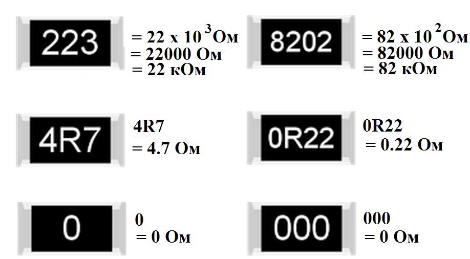
If there are three or four digits in the code, then the last digit means the number of zeros, in fig. 5. The resistor with the code "223" has the following resistance: 22 (and three zeros on the right) Ohm = 22000 Ohm = 22 kOhm. The resistor with the code "8202" has a resistance: 820 (and two zeros on the right) Ohm = 82000 Ohm = 82 kOhm.
In some cases, the marking is alphanumeric. For example, a resistor coded 4R7 has a resistance of 4.7 ohms, and a resistor coded 0R22 has a resistance of 0.22 ohms (here, the letter R is the separator character).
There are also resistors of zero resistance, or jumper resistors. Often they are used as fuses.
Of course, you can not remember the code designation system, but simply measure the resistance of the resistor with a multimeter.
Rice. 5 Marking chip resistors
Ceramic SMD Capacitors
Externally, SMD capacitors are very similar to resistors (see Fig. 6.). There is only one problem: they do not have a capacitance code, so the only way to determine it is to measure it with a multimeter that has a capacitance measurement mode.
SMD capacitors are also available in standard sizes, usually similar to resistor sizes (see above).

Rice. 6. SMD ceramic capacitors
Electrolytic SMS Capacitors

Fig.7. Electrolytic SMS Capacitors
These capacitors are similar to their output counterparts, and the markings on them are usually explicit: capacitance and operating voltage. A strip on the "hat" of the capacitor marks its negative terminal.
SMD transistors

Fig.8. SMD transistor
Transistors are small, so it is impossible to write their full name on them. They are limited to code marking, and there is no international standard for designations. For example, the code 1E may indicate the type of transistor BC847A, or maybe some other. But this circumstance absolutely does not bother either manufacturers or ordinary consumers of electronics. Difficulties can only arise during repairs. Determining the type of transistor installed on a printed circuit board without the manufacturer's documentation for this board can sometimes be very difficult.
SMD Diodes and SMD LEDs
Photos of some diodes are shown in the figure below:

Fig.9. SMD Diodes and SMD LEDs
On the body of the diode, the polarity must be indicated in the form of a strip closer to one of the edges. Usually the cathode output is marked with a stripe.
The SMD LED also has a polarity, which is indicated either by a dot near one of the pins, or in some other way (for details, see the component manufacturer's documentation).
It is difficult to determine the type of SMD diode or LED, as in the case of a transistor: an uninformative code is stamped on the diode case, and most often there are no marks on the LED case at all, except for the polarity mark. Developers and manufacturers of modern electronics care little about its maintainability. It is understood that the repair of the printed circuit board will be a service engineer who has complete documentation for a particular product. Such documentation clearly describes where a particular component is installed on the printed circuit board.
Installation and soldering of SMD components
SMD assembly is optimized primarily for automatic assembly by special industrial robots. But amateur radio amateur designs can also be made on chip components: with sufficient accuracy and care, you can solder parts the size of a grain of rice with the most ordinary soldering iron, you only need to know some subtleties.
But this is a topic for a separate large lesson, so more details about automatic and manual SMD editing will be discussed separately.
In general, the term SMD (from the English. Surface Mounted Device) can be attributed to any small-sized electronic component designed to be mounted on the surface of the board using SMT technology (surface mount technology).
SMT technology (from the English. Surface mount technology) was developed in order to reduce the cost of production, increase the efficiency of manufacturing printed circuit boards using smaller electronic components: resistors, capacitors, transistors, etc. Today we will consider one of these - SMD resistor.
SMD resistors
SMD resistors- These are miniature, designed for surface mounting. SMD resistors are significantly smaller than their traditional counterpart. They are often square, rectangular, or oval in shape, with a very low profile.
Instead of the wire leads of conventional resistors, which are inserted into holes in the PCB, SMD resistors have small contacts that are soldered to the surface of the resistor body. This eliminates the need to make holes in the printed circuit board, and thus allows more efficient use of its entire surface.
Sizes of SMD resistors
Basically, the term frame size includes the size, shape, and pin configuration (package type) of an electronic component. For example, the configuration of a conventional chip that has a flat package with two pins (perpendicular to the plane of the base) is called a DIP.
Size of SMD resistors are standardized and most manufacturers use the JEDEC standard. The size of SMD resistors is indicated by a numerical code, for example, 0603. The code contains information about the length and width of the resistor. So in our example, code 0603 (in inches), the case is 0.060 inches long by 0.030 inches wide.
The same size resistor in the metric system will have code 1608 (in millimeters), respectively, the length is 1.6 mm, the width is 0.8 mm. To convert the dimensions to millimeters, it is enough to multiply the size in inches by 2.54.
Sizes of SMD resistors and their power
The size of the SMD resistor depends mainly on the required power dissipation. The following table lists the sizes and specifications of the most commonly used SMD resistors.

Marking SMD resistors
Due to the small size of SMD resistors, it is almost impossible to apply traditional resistor color markings to them.
In this regard, a special marking method was developed. The most common marking contains three or four numbers, or two numbers and a letter, which has the name EIA-96.
Marking with 3 and 4 digits
In this system, the first two or three digits indicate the numerical value of the resistance of the resistor, and the last digit indicates the multiplier. This last digit indicates the power to which 10 must be raised to get the final multiplier.


A few more examples of determining resistance within this system:
- 450 \u003d 45 x 10 0 is equal to 45 ohms
- 273 \u003d 27 x 10 3 is equal to 27000 ohms (27 kOhm)
- 7992 \u003d 799 x 10 2 is equal to 79900 ohms (79.9 kOhm)
- 1733 \u003d 173 x 10 3 is equal to 173000 ohms (173 kOhm)
The letter “R” is used to indicate the position of the decimal point for resistance values below 10 ohms. Thus, 0R5 = 0.5 ohm and 0R01 = 0.01 ohm.

SMD resistors of increased accuracy (precision), combined with small sizes, have created a need for a new, more compact marking. In this regard, the EIA-96 standard was created. This standard is for resistors with a resistance tolerance of 1%.

This marking system consists of three elements: two digits indicate the code, and the letter following them determines the multiplier. The two digits are a code that gives a three-digit resistance number (see table)
For example, code 04 means 107 ohms and 60 means 412 ohms. The multiplier gives the final value of the resistor, for example:
- 01A = 100 ohm ±1%
- 38C = 24300 Ohm ±1%
- 92Z = 0.887 ohm ±1%

Online SMD resistor calculator
This calculator will help you find the resistance value of SMD resistors. Just enter the code written on the resistor and its resistance will be displayed at the bottom.
The calculator can be used to determine the resistance of SMD resistors that are marked with 3 or 4 digits, as well as according to the EIA-96 standard (2 digits + letter).
Although we have done our best to test the function of this calculator, we cannot guarantee that it calculates the correct values for all resistors, as sometimes manufacturers may use their own custom codes.
Therefore, to be absolutely sure of the resistance value, it is best to additionally measure the resistance with a multimeter.
In our turbulent age of electronics, the main advantages of an electronic product are small dimensions, reliability, ease of installation and dismantling (disassembly of equipment), low energy consumption and convenient usability ( from English- Ease of use). All these advantages are by no means possible without surface mount technology - SMT technology ( S face M ount T echnology), and of course, without SMD components.
What are SMD components
SMD components are used in absolutely all modern electronics. SMD ( S face M ounted D evice), which is translated from English as “surface-mounted device”. In our case, the surface is a printed circuit board, without through holes for radio elements:
In this case, SMD components are not inserted into the board holes. They are soldered onto the contact tracks, which are located directly on the surface of the printed circuit board. In the photo below, there are tin-colored contact pads on the board of a mobile phone that used to have SMD components.

Advantages of SMD components
The biggest advantage of SMD components is their small size. In the photo below, simple resistors and:


Due to the small dimensions of SMD components, developers have the opportunity to place a larger number of components per unit area than simple output radio elements. Consequently, the mounting density increases and, as a result, the dimensions of electronic devices are reduced. Since the weight of the SMD component is several times lighter than the weight of the same simple output radio element, the mass of the radio equipment will also be many times lighter.

SMD components are much easier to desolder. For this we need a hair dryer. How to solder and solder SMD components, you can read in the article how to solder SMD correctly. Soldering them is much more difficult. In factories, they are placed on a printed circuit board by special robots. No one welds them manually in production, except for radio amateurs and radio equipment repairmen.
Multilayer boards
Since in equipment with SMD components there is a very dense installation, there should be more tracks in the board. Not all tracks fit on the same surface, so printed circuit boards make multilayer. If the equipment is complex and has a lot of SMD components, then there will be more layers in the board. It's like a layered cake. The printed tracks connecting the SMD components are located right inside the board and cannot be seen in any way. An example of multilayer boards is mobile phone boards, computer or laptop boards (motherboard, video card, RAM, etc.).
In the photo below, the blue board is Iphone 3g, the green board is the computer motherboard.


All radio repairers know that if you overheat a multilayer board, it will swell up with a bubble. In this case, the interlayer connections are torn and the board becomes unusable. Therefore, the main trump card when replacing SMD components is the right temperature.
On some boards, both sides of the printed circuit board are used, while the mounting density, as you understand, is doubled. This is another plus of SMT technology. Oh yes, it is also worth considering the fact that the material for the production of SMD components takes many times less, and their cost in mass production in millions of pieces costs, literally, a penny.
Main types of SMD components
Let's look at the main SMD elements used in our modern devices. Resistors, capacitors, low-value inductors, and other components look like ordinary small rectangles, or rather, parallelepipeds))

On boards without a circuit, it is impossible to know whether it is a resistor, or a capacitor, or even a coil. The Chinese mark as they want. On large SMD elements, they still put a code or numbers to determine their belonging and denomination. In the photo below, these elements are marked in a red rectangle. Without a diagram, it is impossible to say what type of radio elements they belong to, as well as their denomination.

Sizes of SMD components can be different. Here is a description of the sizes for resistors and capacitors. Here, for example, is a rectangular yellow SMD capacitor. They are also called tantalum or simply tantalum:

And this is what SMD looks like:


There are also these types of SMD transistors:

Which have a large denomination, in the SMD version they look like this:


And of course, how could it be without microcircuits in our age of microelectronics! There are a lot of SMD chip package types, but I mainly divide them into two groups:
1) Microcircuits, in which the leads are parallel to the printed circuit board and are located on both sides or along the perimeter.

2) Microcircuits, in which the conclusions are located under the microcircuit itself. This is a special class of microcircuits called BGA (from English ball grid array- an array of balls). The conclusions of such microcircuits are simple solder balls of the same size.
In the photo below, the BGA microcircuit and its reverse side, consisting of ball leads.

BGA chips are convenient for manufacturers in that they greatly save space on the printed circuit board, because there can be thousands of such balls under any BGA chip. This greatly simplifies the life of manufacturers, but does not make life easier for repairmen.
Summary
What do you use in your designs? If your hands are not shaking, and you want to make a small radio bug, then the choice is obvious. But still, in amateur radio designs, dimensions do not particularly play a big role, and soldering massive radio elements is much easier and more convenient. Some radio amateurs use both. Every day more and more new chips and SMD components are being developed. Smaller, thinner, more reliable. The future, unambiguously, belongs to microelectronics.